Summary
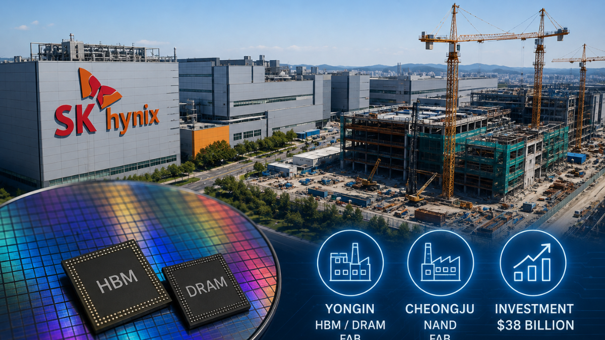
If you're tracking the high-stakes AI hardware race, you need to understand the sheer scale of SK Hynix's latest capital play. The memory giant's board just cleared a massive 54.3 trillion won ($38.30 billion) spending package to build next-generation fabs in South Korea. As an enterprise buyer or tech investor, you'll see this capital split between two key projects. The firm is pouring 35.2 trillion won into the "Y2 fab" at the Yongin semiconductor cluster to ramp up advanced DRAM. Meanwhile, they're directing 19.1 trillion won to build the M17 NAND facility in Cheongju. These investments aim directly at the soaring global demand for High Bandwidth Memory (HBM) and enterprise storage. By locking down these cleanrooms, the company plans to cement its grip on the global hardware supply chain. If you hold their stock, you should also expect fresh capital management updates later this year.
Introduction & Core News Development
If you watch the global silicon markets, you know that keeping up with AI demands an extraordinary amount of cash. You can't just build a software model; you need physical infrastructure to run it. South Korea’s SK Hynix recently confirmed that its board of directors cleared a historic 54.3 trillion won capital spending plan. This decision greenlights the physical construction of fabs that will shape the global AI computing power supply chain for the next decade.
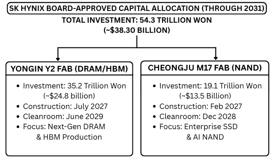
SK Hynix will invest 54.3 trillion won ($38.3 billion) through 2031 to expand its Yongin DRAM/HBM and Cheongju NAND fabrication plants, reinforcing next-generation AI memory manufacturing and long-term semiconductor production capacity.
Let's look at how the board is allocating this cash. You'll see that 35.2 trillion won goes directly to the second phase of development at the Yongin semiconductor cluster. This specific fund will build the "Y2 fab," designed as a manufacturing powerhouse for next-generation Dynamic Random Access Memory (DRAM). The remaining 19.1 trillion won will fund the M17 chip plant in Cheongju. That focuses entirely on NAND flash memory production. If you manage corporate storage networks or deploy hyperscale data centers, this dual-track investment tells you everything you need to know about how the company plans to balance fast processing memory with high-density storage capacity.
Background & Industry Context
To understand why this is happening now, you've to look back at the broad-ranging commitments SK Hynix made earlier. In mid-2024, the chipmaker announced a long-term vision to invest 120 trillion won in the Yongin cluster and another 100 trillion won in Cheongju. The board's recent vote isn't just a routine update; it's the formal, legally binding authorization needed to turn those high-level promises into active construction sites.
This massive spending program fits directly into South Korea’s wider strategy to build a national semiconductor mega-cluster. As you monitor global chip stocks, you'll quickly notice that domestic infrastructure development has become a matter of national economic survival. South Korea's government is coordinating massive public-private initiatives to make sure its local manufacturers aren't left behind by regional rivals. The Yongin cluster is the center of this effort. It's designed to co-locate chip design firms, raw material suppliers, and manufacturing facilities in a single, high-efficiency zone.
Technical Breakdown & Architecture
As a technical analyst or hardware engineer, you'll want to look closely at the specific manufacturing timelines and product focuses of these facilities. The Yongin Y2 fab works to produce advanced DRAM, targeting next-generation architectures like HBM3e and HBM4.
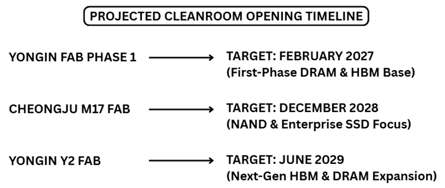
SK Hynix's expansion roadmap outlines cleanroom openings from 2027 to 2029, supporting increased production of DRAM, HBM, NAND flash, and enterprise SSDs to meet rising AI semiconductor demand.
In the semiconductor world, a cleanroom is a highly controlled environment where air filtration, temperature, and humidity are managed to prevent microscopic particles from ruining silicon wafers. You can trace the planned rollout through these key phases:
- Yongin Fab Phase 1: Construction is already well underway. You can expect the first cleanroom here to open in February 2026.
- Yongin Y2 Fab: Construction is scheduled to begin in July 2025. You'll see the first cleanroom open in June 2029, focusing on high-bandwidth memory.
- Cheongju M17 Fab: Construction will start in February 2027. The company expects to open this cleanroom in December 2028 to ramp up advanced NAND flash production.
When you look at HBM architecture, you're looking at vertically stacked DRAM dies connected by Through-Silicon Vias (TSVs). This design bypasses the physical space limitations of traditional motherboard layouts. By placing the memory stack directly next to the GPU or specialized accelerator, you get much wider data buses and lower power consumption. The M17 fab in Cheongju will apply a similar vertical focus to NAND storage, using advanced 3D stacking techniques to pack more terabytes into enterprise-grade solid-state drives (SSDs). And fast.
Business Impact & Strategic Implications
If you run data centers or buy enterprise servers, this massive CapEx program will directly affect your future hardware costs. This level of spending is necessary to secure semiconductor supply deals with major AI chip designers who need guaranteed access to high-performance memory. Few saw this coming.
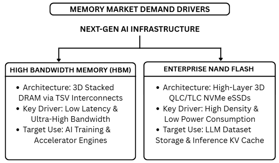
The AI infrastructure boom is driving demand for two critical memory technologies: High Bandwidth Memory (HBM) for AI training and Enterprise NAND Flash for large-scale data storage and inference workloads.
But as an investor, you've to weigh these huge capital demands against near-term shareholder value. Building advanced fabs requires billions of dollars upfront before a single wafer is sold. That can put pressure on short-term cash flow. To address these concerns, SK Hynix announced in a regulatory filing that it's actively reviewing updated shareholder return policies. You can expect the details of this capital management plan to be finalized and shared during the company's third-quarter earnings announcement, as they look to keep investors confident while funding these long-term projects.
Industry Perspective & Ecosystem Dynamics
When you step back to look at the global market, you'll see this investment is part of a larger race to secure supply lines for AI hardware. The memory market is highly consolidated, and SK Hynix is using its early lead in HBM3e production to secure a strong position with key system designers.
By building out the Yongin cluster, SK Hynix is positioning itself alongside South Korea's AI infrastructure initiatives. This aligns them with global supply requirements, especially as major cloud providers work to diversify their hardware options. Hardly.
Meanwhile, domestic competitors are moving quickly. You can see this in how Samsung is pushing forward its own semiconductor wafer fab plans to match these timelines. Also, emerging global suppliers are looking to capture more of the market, as shown by recent high-volume DRAM supply agreements in regional markets. This competitive market means that any delay in building cleanrooms or upgrading lithography equipment could cause a company to quickly lose market share.
GlobalByte Perspective
If you look past the massive numbers, you'll see that this $38 billion plan is a calculated gamble on the long-term growth of the AI sector. The semiconductor industry has always gone through sharp boom-and-bust cycles, and building these massive cleanrooms years before they run at full capacity carries real risk. If the growth in AI infrastructure demand slows down over the next three to five years, you could see a market with too much high-bandwidth memory capacity. This oversupply would likely drive down prices and squeeze corporate profit margins.
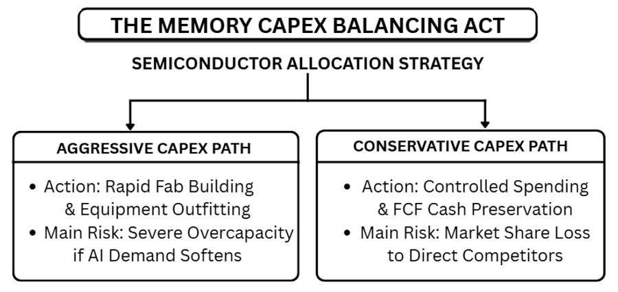
Semiconductor manufacturers face a strategic trade-off between accelerating AI-driven capacity expansion and preserving financial flexibility, balancing growth opportunities against the risks of overcapacity and increased competitive pressure.
But the risk of underinvesting is even higher for SK Hynix. If you don't build out these facilities now, you risk losing your position as a primary supplier to major AI chip designers. By committing to both Yongin and Cheongju, the company is preparing for a future where both high-speed computation (DRAM/HBM) and high-capacity storage (NAND) are co-dependent bottlenecks in deep learning systems. As you watch this roll out, your main focus should be on how well they manage these construction timelines without letting yields fall or allowing engineering talent to drift to competitors. Here’s why.
Future Outlook & Strategic Roadmap
As you look ahead, the success of this capital plan will depend on meeting a series of strict construction and licensing milestones. The first major milestone to watch is the opening of the initial Yongin cleanroom in early 2026. This will show how well the local infrastructure can support high-volume manufacturing. Case in point.
On the ground, these developments will test the local utility grids and supply networks. The AI chip hub in Yongin requires massive amounts of electrical power and clean water to run its advanced lithography equipment. If you're tracking these projects, you should pay close attention to South Korea's regional energy and water planning. Any delay in building out the local power grid or water pipelines will directly push back the 2029 production targets for the Y2 fab, shifting the balance of the global memory market.