If you've been tracking China's AI hardware push, the constraints aren't theoretical. Access to TSMC's most advanced process nodes is blocked. US export controls have drawn a hard line. And AI models keep growing - demanding more memory bandwidth, more compute density, more of everything that planar chip design struggles to deliver at scale.
This is why Chinese AI chips’ 3D stacking technology has moved from an engineering alternative to a genuine strategic priority. Instead of chasing process nodes they can't reach, chip makers are stacking dies vertically - putting compute and memory physically closer together to close the gap that flat designs can't.
Why 2.5D Packaging Is Running Out of Road
The "memory wall" isn't a new problem. But AI workloads have made it acute. When a model has hundreds of billions of parameters, the speed at which data moves between memory and compute becomes the bottleneck - not raw processing power.
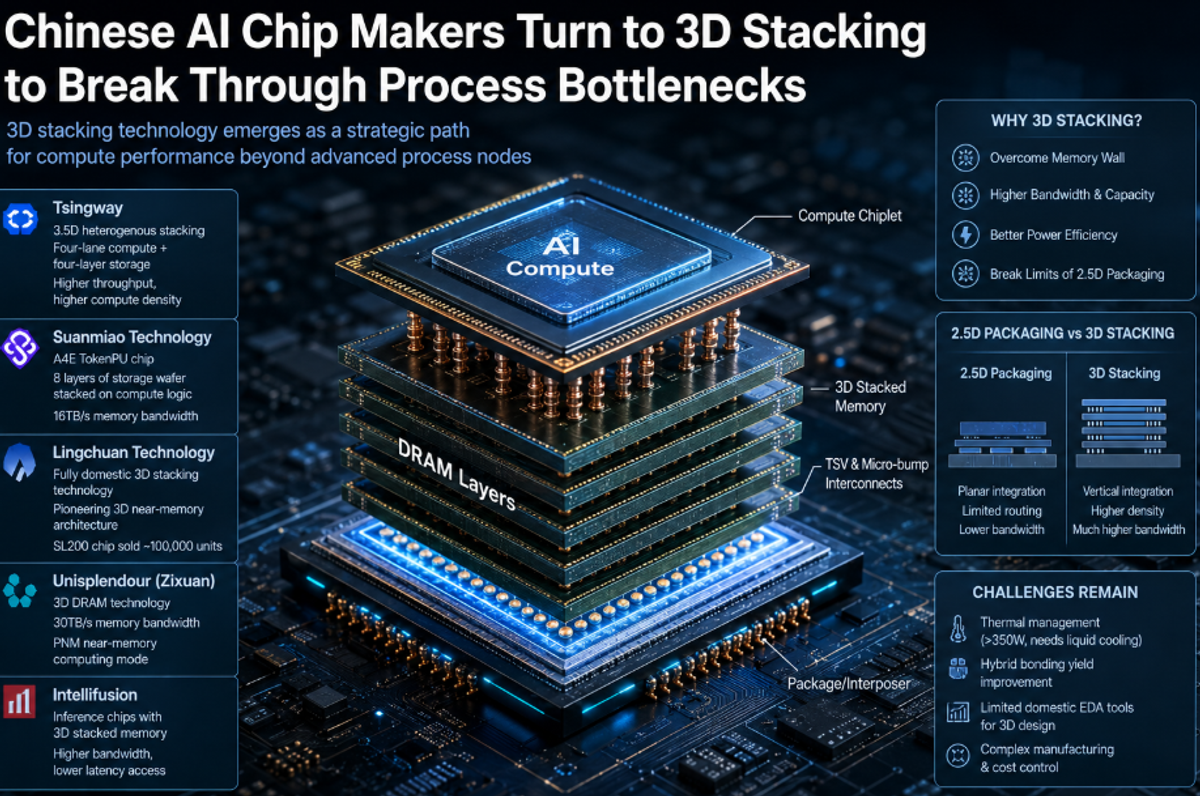
Mainstream 2.5D packaging technologies, including TSMC's CoWoS platform, face fundamental constraints in routing resources and integration density. Why 2.5D packaging technologies face routing constraints in AI workloads comes down to geometry: everything stays flat, which limits how many connections you can fit and how fast data can travel. It works for a lot of use cases. For high-compute AI workloads at scale, it doesn't.
3D stacking solves this by going vertical. Memory sits directly on compute logic. Bandwidth climbs. And you can reach meaningful high compute AI workloads integration density without needing a 2nm process node to get there.
The Companies Actually Building Chinese AI Chips 3D Stacking Technology
Several Chinese firms are well past the whiteboard.
Tsingway is developing its next-generation AI chips using a 3.5D heterogeneous stacking approach - a "four-lane compute plus four-layer storage" spatial architecture that pairs reconfigurable compute chiplets with vertically stacked DRAM for dramatically improved data throughput.
Suanmiao Technology has taped out its A4E TokenPU chip: eight layers of storage wafer vertically stacked on compute logic, achieving 16TB per second memory bandwidth through TSV and micro-bump interconnects. That's already done.
Lingchuan Technology is probably the most commercially compelling story right now. Spun off from Kuaishou, it uses fully domestic 3D stacking technology with a pioneering near-memory architecture. Its SL200 chip has shipped nearly 100,000 units to customers including Alibaba Cloud, Baidu Cloud, and Bilibili. That's not a roadmap - those are real shipments to real cloud customers.
Unisplendour's Zixuan architecture targets 30TB per second memory bandwidth with a PNM near-memory computing mode. Intellifusion is developing inference chips with 3D stacked memory for lower-latency inference workloads specifically.
The broader ecosystem is maturing alongside these chips. The recent CXMT server DRAM supply deal with Tencent signals that domestic memory supply chains are catching up - which is exactly what 3D stacking efforts need to function at scale. And these chips are increasingly destined for the kind of domestic supercomputing platform infrastructure being built alongside them.
The Engineering Problems That Don't Have Easy Answers
None of this is simple.
Stacked dies exceeding 350W require liquid cooling. Most data center infrastructure wasn't designed for it. Overcoming thermal management and liquid cooling challenges for stacked dies is a real operational problem, not an engineering footnote. Improving hybrid bonding yield in domestic semiconductor fabrication is another honest gap - the process that fuses dies together is demanding, and Chinese fabs are still building the accumulated process knowledge needed to do it at high yield.
Then there's domestic EDA tooling for 3D chip design. It lags what TSMC's customers can access. You're designing something structurally more complex with a thinner software toolkit. That adds real time to development cycles.
That said, extreme thermal demands are a cross-sector challenge. China's investment in quantum cooling infrastructure shows the country is tackling cooling problems at multiple levels - some of those solutions will transfer to data center deployments.
What This Means for AI Hardware Strategy
The logic here is clean. If advanced process nodes are out of reach, extract more from the nodes you have. Achieving high compute density independent of process node advancement is the core argument for 3D stacking as a sovereign hardware strategy - and it's a compelling one.
Demand isn't waiting. Meituan's trillion-parameter AI model is a useful reminder of how much compute pressure Chinese AI labs are generating at the application layer. The Chinese AI clusters and trade targets set at the state level make this a policy-level infrastructure priority, not just commercial R&D.
And the ripple extends further. Chinese open-source AI in Africa is already reshaping technology access across the continent. Better hardware means better AI, wherever that AI ends up running.
The Bigger Picture
Chinese AI chips 3D stacking technology isn't a workaround people are settling for. It's becoming the actual strategy - and it's producing real chips with real customer deployments behind them.
The memory wall problem is real. The process node access problem is real. 3D stacking addresses both at once, not perfectly, but genuinely. The engineering hurdles - thermal management, bonding yield, tooling gaps - are also real, and none of them are trivial to solve.
But the chips are shipping.
For more on where all of this fits in China's broader semiconductor story, the science and semiconductor coverage is worth following closely.