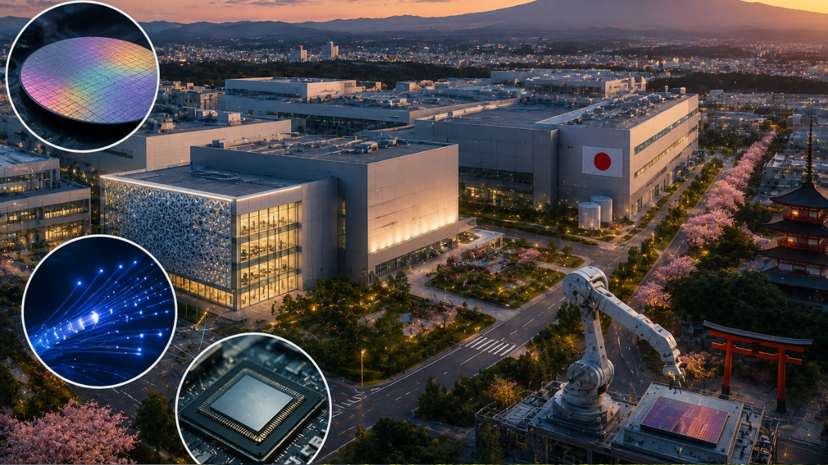
Tower Semiconductor's Japan fab expansion Silicon Photonics METI announcement, dropped July 14, 2026, isn't a routine capacity increase. The company is committing roughly $3 billion to a dual-track build across its Japanese operations - net of a $1 billion government grant - focused on scaling 300mm Silicon Photonics and Silicon Germanium manufacturing to meet AI data center demand that existing capacity simply can't cover.
Here's what that actually looks like.
Tower Semiconductor's Japan Fab Silicon Photonics METI Expansion: Two Tracks Running at Once
Two things are happening simultaneously.
Track one repurposes the Arai facility, formerly known as Fab 6, for 300mm Silicon Photonics capacity and advanced packaging capabilities, while pushing Fab 7 in Uozu toward its output ceiling. Full production readiness is targeted for Q4 2027. That's fast - compare it to the typical wafer fab construction timeline for greenfield builds, which routinely runs two-plus years longer.
Track two constructs an entirely new 300mm facility adjacent to Fab 7, designed for a multi-fold increase in Silicon Photonics and Silicon Germanium capacity. Agreements are still being finalized, so this part carries real execution uncertainty - but the strategic direction is locked in.
Total investment scope: approximately $3 billion, net of the $1 billion METI grant. Tower is covering $2 billion of that itself. That's a real commitment, not a subsidized press release.
Why Repurposing Arai Comes First
CEO Russell Ellwanger was direct about the logic: converting an existing facility "eliminates the timing concerns and impacts of multi cycles of learning for a greenfield qualification or a fab-to-fab product transfer."
That's not marketing language. Greenfield fabs require multi-year qualification before a single production wafer ships. Existing facilities don't. You keep the trained workforce, skip the ramp delays, and actually deliver to customers on schedule rather than 18 months late. The Arai facility Fab 6 repurposing for 300mm wafer foundry capacity is the lower-risk, faster half of this expansion - and it's where the 2027 timeline comes from.
Tower has done this before. The TPSCo conversion of former Panasonic Semiconductor operations is the template here, and that track record gives the timeline credibility.
Tower Semiconductor's Updated Revenue Targets After the Japan Silicon Photonics METI Build
Numbers are on the table: $3.6 billion in revenue and $1.2 billion in net profit by 2028, driven primarily by track one capacity coming online during 2027. Tower Semiconductor's updated 2028 revenue projections are anchored in multi-generational customer partnerships - customers who've been engaged across multiple design cycles, not speculative demand forecasts built on assumptions.
Track two becomes accretive starting in 2029. It's a second growth phase that extends the financial story well past the initial model update.
Are these guaranteed? No - Tower's disclosures cover demand fluctuation, construction risks, and grant condition covenants. But companies don't publish $3.6 billion revenue targets without substantial customer commitments behind them.
Silicon Germanium: The Other Half Nobody's Focusing On
Everyone's talking about Silicon Photonics. Silicon Germanium advanced packaging capabilities for AI data centers deserve equal attention - and they're getting less of it.
SiGe handles the critical electrical-to-optical signal conversion inside transceivers. As AI cluster interconnect speeds climb toward 400G and 800G, the tolerance for weak conversion components hits zero. You can have the most impressive 3D chip stacking breakthroughs at the compute layer - but a SiGe bottleneck at the optical link cancels most of that gain. Tower's expansion adds SiGe capacity alongside SiPho precisely because the two technologies serve complementary functions in the same optical connectivity hardware stack. You need both.
High-volume foundry SiGe sourcing has been harder to find than most coverage suggests.
Japan's $1 Billion METI Grant Is Industrial Policy, Not Generosity
The METI semiconductor grant for Japan chip manufacturing infrastructure in 2026 isn't charity. It's a deliberate push to establish sovereign advanced packaging and domestic fabrication infrastructure that can absorb supply chain shocks - geopolitical or otherwise.
For anyone following the pressure around overseas semiconductor tech transfers and the risks those create across global supply chains, Japan anchoring advanced SiPho manufacturing domestically reads as a direct policy response. Ellwanger's references to Toyama and Niigata prefectures, local university partnerships, and regional supplier development aren't just optics. Tower has existing roots in both regions through TPSCo, and this expansion deepens them deliberately.
The goal isn't just manufacturing jobs. It's capability that can't be switched off.
Why the Timing Matters for Global AI Hardware
The demand driving this expansion is already here. As firms pivot to local chip suppliers and supply concentration becomes a board-level risk, the need for reliable specialty analog foundry options keeps growing. A chip supply deal reshaping AI can close in weeks - qualifying a foundry process takes months to years. Tower's expanded capacity compresses that gap for customers already on its process platforms.
Nvidia chip purchase limits have pushed hyperscalers to examine component sourcing at every layer of the stack, not just GPUs. Korean fabless chipmakers expanding into new markets need stable analog foundry access across design cycles. DRAM supply chain agreements worth billions are being locked in right now as the industry prepares for the next compute wave - and optical interconnect sourcing is next in that queue.
Heterogeneous computing platforms that tie together compute, memory, and connectivity components depend on optical interconnects hitting both performance and cost targets at volume. Tower's Japan capacity directly serves that need. For IDMs and fabless companies wanting B2B silicon photonics foundry process transfer services without building their own fabs, Tower's expanded footprint - alongside its shared 300mm facility in Italy with STMicroelectronics - provides multi-fab sourcing depth that's rare in this space. Nvidia and Qualcomm at chip expos keep underscoring how central optical connectivity is to next-gen AI hardware. The foundry supply side is finally starting to match that.
The Real Signal in This Announcement
The Tower Semiconductor Japan fab expansion Silicon Photonics METI partnership is, at its core, a timing bet - made with real money on both sides. Silicon Photonics and Silicon Germanium aren't niche analog processes anymore. They're foundational to the AI data center infrastructure being built right now, at scale, and qualified high-volume foundry capacity for them has been running behind demand.
Track one lands in 2027. Track two starts compounding from 2029. The updated business model puts $3.6 billion in revenue on the table by 2028.
For hyperscalers, transceiver manufacturers, and fabless companies watching this space - this isn't just a capacity announcement. It's a supply chain anchor point that was genuinely missing.