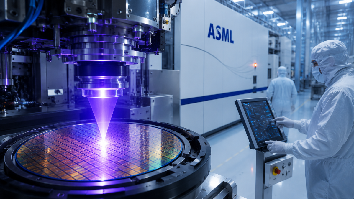
Quietly, but with real significance, Intel has started using one of the world's most expensive machines to build its next flagship laptop processors. Intel Panther Lake ASML High NA EUV lithography - yes, it's a mouthful - but this is a genuine manufacturing milestone with real implications for the chip industry at large.
So let's get into it.
What Is High NA EUV, and Why Does It Cost $400 Million?
Lithography is how chipmakers print the microscopic circuit patterns that make a chip function. You're essentially using light to draw incredibly fine designs onto silicon wafers - patterns so small they operate at the atomic scale. Standard EUV (extreme ultraviolet) machines have been the industry's go-to tool for this for several years.
But as chip features keep shrinking, standard EUV is getting stretched. High NA EUV is the next step.
"High NA" stands for high numerical aperture - a measure of how precisely the machine's optical system captures and focuses light. More precise focus means sharper, finer circuit patterns on the wafer. Think of it like upgrading from a decent camera lens to a professional optic with far greater resolving power.
And the price shows up on the balance sheet. A High NA EUV machine costs around $400 million, roughly twice what a standard EUV unit runs. ASML - the Dutch company that manufactures every one of these machines on the planet - is the sole supplier. That concentration of capability is a big part of why global semiconductor competition has become so fiercely contested.
These machines are also technically challenging to integrate into live production. You can't just plug one in and start running at full speed.
Intel Panther Lake ASML High NA EUV Lithography: What's Actually Happening
Intel's Panther Lake chips - its upcoming flagship laptop processor line - are built using Intel's 18A manufacturing process. That process already relies on ASML's standard EUV lithography machines for most layers. But now, Intel Panther Lake ASML High NA EUV lithography has entered the production flow for specific layers of the chip.
Not all layers. Specific ones.
Intel isn't dismantling its existing workflow. It's adding the High NA tool for targeted portions of the manufacturing process - the layers where finer resolution translates into real gains in feature density or power efficiency. The goal at this stage isn't maximum production volume. It's data collection and systematic optimization of the equipment under real conditions.
Intel received its first High NA machine in 2024 at its Hillsboro, Oregon research and development facility - the site where Intel validates new manufacturing techniques before scaling them to high volume. This kind of methodical, unglamorous validation work, similar to what's driving next-gen wafer fab construction projects elsewhere in the world, is how R&D eventually becomes production reality.
Experiments started in 2024. What's happening now with Panther Lake is those experiments graduating into actual chips.
The Economic Debate Nobody Has Fully Settled
Here's the thing: the chipmaking world hasn't agreed on when deploying High NA EUV actually makes economic sense.
The case for early adoption is clear enough. As chips shrink further, standard EUV - even with multi-patterning techniques that run the machine in multiple passes to achieve finer resolution - will hit practical limits. High NA EUV is the cleaner long-term path to next-generation extreme ultraviolet lithography microchip printing. But "eventually necessary" doesn't automatically mean "necessary right now."
The case for waiting is also real. At $400 million per machine, with significant technical integration challenges and a steep learning curve ahead, the economics only work when you're running at high throughput and high yield. Getting there takes time that not everyone has been willing to spend yet.
Intel has come down on the side of early adoption - partly because the broader semiconductor supply chain shifts unfolding globally make forward positioning more valuable than it used to be. Chipmakers without access to High NA EUV have had to explore 3D chip stacking workarounds and heterogeneous chip architectures instead. Those approaches work. But they're workarounds, and everyone in the industry knows it.
Why Intel Is Moving Now
Intel declined to comment on the announcement publicly. Not unusual.
But the reasoning isn't hard to reconstruct. Intel's been working to reclaim its standing as a manufacturing leader, and the 18A process is central to that story. Integrating High NA EUV into Panther Lake chip production - even at the layer level - isn't just about improving those specific chips. It's about building institutional knowledge. Intel and ASML both get real production data from these runs. Both sides learn how to optimize the equipment under actual manufacturing conditions, not just controlled tests.
That knowledge compounds. The cutting-edge chip development race is fundamentally a learning race. Getting fluent in High NA EUV now, even at limited scale, gives Intel expertise that later entrants will spend years trying to replicate.
There's also geopolitical weight here. High NA EUV machines are subject to strict semiconductor technology export rules that limit their availability in certain markets. Nations and companies facing advanced chip access restrictions simply can't build the same depth of lithography expertise. How much that translates into durable long-term advantage won't be clear for several years - but the gap is real and widening.
What Intel Panther Lake ASML High NA EUV Lithography Means for the Industry
Next-generation extreme ultraviolet lithography is where advanced microchip printing is unambiguously heading. Intel Panther Lake ASML High NA EUV lithography represents the first publicly confirmed instance of this tool moving from R&D into a real flagship processor manufacturing line - even if partially, even if at limited volume today.
It fits into a larger domestic chip production push taking shape across the US semiconductor sector, and it's quietly reshaping shifting chip supply dynamics on a global scale. The companies that build genuine production fluency with these tools now - not just access, but hard-won manufacturing expertise - will be best positioned when High NA EUV stops being optional.
That's not a trivial bet at $400 million a machine.